Blog Entry
Controlling DC motor with AVR ATtiny13 PWM and ADC Project
December 27, 2008 by rwb, under Microcontroller.
It’s interesting to explore what we can do with this tiny 8 pins; 8-bit microcontroller. The ATtiny13 is the smallest and cheapest Atmel AVR 8-bit microcontroller families but yet, it’s loaded with sophisticated peripherals such as two 8-bit PWM channels and 4 channels 10-bit ADC. Although the memory is quite small; 1 K flash, 64 SRAM and 64 EEPROM but this more the adequate for most PWM and ADC application, if you need more memory, bellow is the list of other Atmel AVR 8 pins microcontrollers which have compatible pins with ATtiny13 microcontroller.

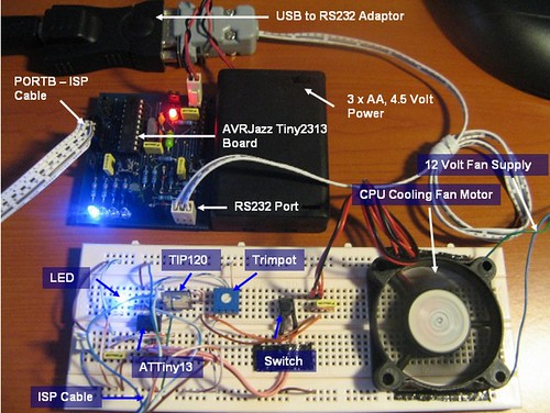
In order to demonstrate the ATtiny13 microcontroller capabilities using both PWM and ADC, I decided to use it for controlling the motor speed, after searching for the right motor for this project, finally I’ve found a microprocessor cooling fan from my old Intel Celeron computer; so I think this is a perfect motor for this project. By connecting it to the TIP120 Darlington pair transistor and to the ATtiny13 OC0A output we could easily controlling this fan speed using PWM, bellow is the complete schema for this project:

The 10K trimpot is used as an input for ADC which connected to the ADC1 input on the ATtiny13 (PIN 7) and to make it little bit more interesting I added the switch (S1) for switching the fan on/off and LED for the program life beacon, this LED will blink according to the PWM value passed to the fan, if the fan rotate faster the LED will blink slowly, but when the fan rotate slower the LED will blink faster. The fan speed is controlled by the trimpot which works as a voltage divider that supply the variable voltage to the ATtiny13 analog input.
The following is the list of hardware and software I use in this project:
- 3 Resistors: 2K7, 10K (2 pieces), 300 Ohm
- 1 Trimport: 10K
- 2 Capactors: 100nF, 1 capacitor: 10nF
- 1 Diode: 1N4001
- 1 LED
- AVR ATtiny13 microcontroller
- 1 TIP 120 Darlington pair transistor
- One 12 Volt DC motor
- AVRJazz Tiny2313 board as the programmer board from ermicro
- OvrOspII programmer software from Mike Henning
- Atmel AVR Studio 4 for the coding, compiling and debugging environment
The Tiny Code
To program the ATtiny13; this time I choose to use AVR’s assembler instead of C, because I just want to make sure that everything will feed into this tiny 1K flash boundary and just curiously how big this code will be; Ok let’s take a look in this assembler code bellow:
;*********************************************************************
; Program		: t13pwm.asm
; Description		: Tiny13 Fast PWM and ADC Fan Controller
; Last Updated	        : 15 December 2008
; Author		: RWB
; IDE/Compiler  	: Atmel AVR Studio 4.14
; Programmer    	: AvrOspII v5.47 from Mike Henning
;               	: AVRJazz Tiny2313 Board
;*********************************************************************
.include "tn13def.inc"
; The Tiny13 Default Frequency Clock
.equ F_CPU = 9600000
.cseg
; Start on the flash ram's address 0
.org 0
main:   ldi R24,RAMEND         ; Initial Stack Pointer
	out SPL,R24            ; SP = RAMEND
; Initial I/O
        ldi   R16,0b00010011   ; Set PB0=Output, PB1=Output, PB2=Input, PB3=Input, PB4=Output
        out   DDRB,R16         ; DDRB=0x13
; Initial ADC
        ldi   R16,0b10000110
	out   ADCSRA,R16       ; Turn On the ADC, with prescale 64
	ldi   R16,0b00000000
	out   ADCSRB,R16       ; Free running mode
	ldi   R16,0b01100001
	out   ADMUX,R16        ; Internal Reference 1.1 Volt,Left Adjust, Channel: PB2 (ADC1)
	ldi   R16,0b00000100   ; Disable Digital Input on PB2
	out   DIDR0,R16
; Initial PWM
        ldi   R16,0b10000011
 	out   TCCR0A,R16       ; Fast PWM Mode, Clear on OC0A
	ldi   R16,0b00000100
	out   TCCR0B,R16       ; Used fclk/256 prescale
; Initial the Button Flag and PORTB
	ldi   R17,0            ; Initial Button Flag
        out   PORTB,R17

lb_00:  sbic  PINB,PB3         ; if (PB3 == 0)
        rjmp  lb_20            ; else goto lb_20
        ldi   R19,5            ; Use delay for simple debounce
  	rcall delay_func
	sbic  PINB,PB3         ; if (PB3 == 0), read again
        rjmp  lb_20            ; else goto lb_20
	cpi   R17,1            ; Process if button pressed
	brne  lb_10            ; if (R17 != 1) goto lb_10
	ldi   R17,0            ; else R17=0
	ldi   R16,0            ; Disable PWM Clock
        out   TCCR0A,R16       ; TCCR0A = 0
	out   TCCR0B,R16       ; TCCR0B = 0
	cbi   PORTB,PB0        ; Turn off Motor
	cbi   PORTB,PB1        ; Turn off LED
        rjmp  lb_20
lb_10:	ldi   R17,1	       ; R17=1
        ldi   R16,0b10000011
	out   TCCR0A,R16       ; Fast PWM Mode, Clear on OCR0A
	ldi   R16,0b00000100
	out   TCCR0B,R16       ; Used fclk/256 prescale
        sbi   PORTB,PB1        ; Turn on LED

lb_20:  cpi   R17,1            ; if (R17 != 1)
	brne  lb_40            ; goto lb_50
				            ;
        sbi   ADCSRA,ADSC      ; Start ADC conversion
lb_30:  sbic  ADCSRA,ADSC      ; while (ADCSRA & (1<<ADSC))
	rjmp  lb_30
	in    R16,ADCH         ; Read the result Ignore the last 2 bits in ADCL
        out   OCR0A,R16        ; OCR0A = R16
        cbi   PORTB,PB1        ; Turn off LED
	mov   R19,R16
	rcall delay_func       ; Call Delay Function Parameter R19
        sbi   PORTB,PB1        ; Turn on LED
lb_40:	mov   R19,R16
	rcall delay_func       ; Call Delay Function Parameter R19
     	rjmp  lb_00
; Simple Delay Function
delay_func:
delay0: ldi   R20,25           ; R20 = 25
delay1: ldi   R21,255          ; R21 = 255
delay2: dec   R21              ; Decrease R21
	brne  delay2           ; if (R20 != 0) goto delay2 label
        dec   R20              ; Decrease R20
        brne  delay1           ; if (R20 != 0) goto delay1 label
	dec   R19              ; Decrease R19
	brne  delay0           ; if (R19 != 0) goto delay0 label
	ret                    ; Return to the caller
.exit
The first statement groups in the main area is to initial the stack, the stack use the microcontroller SRAM memory and we put the stack pointer to the end of 64 byte boundary (RAMED), the next statement groups is to initial the data direction register on the PORTB and make the direction as the following tables:

Analog to Digital Conversion Initialization
The next statements group is to initiate the ADC peripheral on the ATtiny13 microcontroller (please see the datasheet for complete explanation). To use the ADC peripheral we use these following steps:
A. Select the prescaler and activate the ADC peripheral
Prescale device is used to prescale the clock frequency (internal or external) and this clock is used by the successive approximation circuitry inside the ADC peripheral to convert the analog signal. To get the maximum resolution we could choose the frequency between 50 kHz to 200 kHz, in this project I use 64 prescale; therefore the frequency is about 150 kHz (9600000 Hz / 64).


Because we are not using the auto trigger (ADATE) and interrupt ADC (ADIF and ADIE) then we can set these bits off, so by selecting 64 prescaler (ADPS2, ADPS1 and ADPS0) and enable the ADC peripheral (ADEN) we assign the ADC Status and Control register as follow:
ldi   R16,0b10000110
out   ADCSRA,R16       ; Turn On the ADC, with prescale 64
B. Select the ADC trigger sources
We use the free running mode trigger source, means the ADC peripheral always do the conversion when we instruct to start the ADC conversion:


Therefore by setting the ADC trigger source bits (ADTS2, ADT21 and ADTS0) to logical “0” we instruct the ADC peripheral to run in free running mode:
ldi   R16,0b00000000
out   ADCSRB,R16       ; Free running mode
C. Select the ADC channels
We have to tell to the ADC peripheral which ADC port we are going to use by selecting the multiplexer bits MUX1 and MUX0 in ADC multiplexer selection register (ADMUX):


From the above table the ADC1 (PB2) channels used in this project is set by assigning bits MUX1=0 and MUX0=1. Next we will choose the 1.1 volt internal reference voltage by setting the voltage reference bit (REFS0) to logical “1“:

When the ADC peripheral finish converting, it will place the result in ADC data register pairs ADCH and ADCL; because in this project we just use the 8-bit conversion, we set to left adjust the ADC result by setting the bit ADLAR to logical “1” in the ADMUX register and read the result only in the ADCH register (we just ignore the LSB bits in the ADCL register).
ldi   R16,0b01100001
out   ADMUX,R16     ; Reference 1.1 Volt, Left Adjust, Channel: PB2
D. Disabling the digital input on the Analog Channel
The last initiation process is to disable the digital input on the analog channel (ADC1) we use to reduce the power consumption in the digital input buffer:

By setting the ADC1D digital input to logical “1“, we disable the digital capability on port PB2:
ldi   R16,0b00000100   ; Disable Digital Input on PB2
out   DIDR0,R16
Pulse Width Modulation Initialization
The ATtiny13 has two independent PWM channels output one is OC0A (PB0) port that we used in this project and the other is OC0B (PB1) port. To activate the PWM peripheral in ATtiny13 microcontroller we use these following steps:
A. Choosing the waveform generation mode
The ATtiny13 microcontroller support two types of PWM mode; first is the fast PWM mode which is provide high frequency output, the second one is the phase correct PWM mode which is base on dual slope counter operation; this type of PWM mode has lower frequency output comparing to the fast PWM mode. In this project we will use the fast PWM mode.


By setting the COM0A1=1 and COM0A0=0, we choose the clear OC0A on compare match, set OC0A on top. This mean when the TCNT0 counter register equal to the OCR0A register value then the output of OC0A (PB0) will be logical “0” and when the TCNT0 reach the maximum value (255) then the output of OC0A will be logical “1“. The fast PWM mode could be choose by setting the WGM2=0 bit in TCCR0B register, WGM1=1 and WGM2=1 bits in TCCR0A register.
ldi   R16,0b10000011
out   TCCR0A,R16       ; Fast PWM Mode, Clear on OC0A
B. Choosing the counter frequency
The heart of PWM peripheral lays in the 8-bit timer/counter, when we start the counter the wave generation form circuit will continue comparing the TCNT0 counter register value with the OCR0A register value and generating the output base on this comparison result. In order to activate the counter we need to supply the clock to the counter which can be choose from the prescaler device inside the timer/counter peripheral.


In this project I used the 256 prescaler, means the Fast PWM frequency generated by the waveform generator can be calculated using this following formula:
![]()
Where N is the prescaler, therefore the output frequency on OC0A with 9.6 Mhz internal clock will be
fOC0A=9600000 / (256 x 256) = 146.48 Hz
You should experiment with your own prescaler factor which is depends on the DC motor you use. Try to start with big prescaler first and slowly decrease it and see how your DC motor response. The force output compare bits FOC0A and FOC0B in register TCCR0B is set to logical “0” in PWM mode.
ldi   R16,0b00000100
out   TCCR0B,R16       ; Used fclk/256 prescale
Inside the Code
Basically the code is self explained (I put a lot of comments inside it), but I want to explain it with the C style pseudo code so hopefully you will have better understanding of how the program works:
Initial_PORTB();
Initial_ADC();
Initial_PWM();
R17_SwicthFlag = 0;
for(;;) {
  if (switch_PB3_is_pressed()) {
    if (R17_SwicthFlag == 0) {
      R17_SwicthFlag = 1;
      Enable_PWM();
      Turn_On_LED();
    } else {
      R17_SwicthFlag = 0;
      Disable_PWM();
      Turn_Off_LED();
    }
  }
  if (R17_SwicthFlag == 1) {
    Enable_ADC();
    Wait_ADC_Conversion();
    PWM_OC0A = ADC_Result_in_ADCH;
    Turn_Off_LED();
    Delay(ADC_Result_in_ADCH);
    Turn_On_LED()
  }
  Delay(ADC_Result_in_ADCH);
}
From the pseudo code you could see the endless loop inside the for(;;) statement is similar to the assembler syntax bellow:
lb_00: sbic PINB,PB3
        ...statement
        ...statement
        ...statement
rjmp lb_00
Inside this endless loop we do the switch reading, PWM enable and disable, ADC conversion, LED on and off.
By setting the ADSC bit to logical “1” in ADCSRA register we instruct the ADC peripheral inside the ATtiny13 to start read the channel (PB2) and start the ADC conversion, then we just wait until this bit is cleared when the ADC conversion is done:
        sbi   ADCSRA,ADSC      ; Start ADC conversion
lb_30:  sbic  ADCSRA,ADSC      ; while (ADCSRA & (1<<ADSC))
	rjmp  lb_30
        in    R16,ADCH         ; Read the result Ignore the last 2 bits in ADCL
        out   OCR0A,R16        ; OCR0A = R16
As I explained before, I use LED indicator for the program life beacon; but to make it interest I put the ADC result value as the delay parameter for the delay function, this make the delay times varied as we adjust the trimpot.
        mov   R19,R16
        rcall delay_func       ; Call Delay Function Parameter R19
When the ADCH value is high means the PWM high pulse (logical “1“) output generated by the waveform generator on the OC0A (PB0) port will be wider this mean the DC motor will turn faster, while the LED delay times will be longer; when the ADCH value is low means the PWM high pulse will be sorter and the DC motor will turn slower but the LED delay times will be sorter. You can change this behavior by changing the COM0A1 and COM0A0 bits setting in the TCCR0A register, this will change the OC0A output.
Loading and Running the Code
After compiling and debugging (you should always go through this procedure) you should get this following result:

The code only occupied about 128 bytes from the total 1024 byte flash, this sound good means there are more space for improvement in the future. As you see the 1K flash of ATtiny13 is still adequate for average PWM and ADC application. Ok let’s down load the code, but before we do that check the ATtiny13 fuse bit setting using the OvrOspII program and should be set as follow:

Make sure you choose the Int. RC Osc. 9.6Mhz; Start-up time: 14 CK + 64ms, after verifying it you are ready to down load the code to the ATtiny13 microcontroller.
The ATtiny13 PWM and ADC project in action:
Notes: when the fan turn slower, the LED blink faster but when captured in the video it appear to blink slower because the blinking is very fast.
Bookmarks and Share


Comment by پروژه الکترونیک.
For controlling direction of the motor a bridge driver must be used, for example L298.