Blog Entry
Stepping Into the 16-bit World with the Microchip 16-bit PIC24F16KA102 Family Microcontroller
May 31, 2010 by rwb, under Microcontroller.
One of the commonly asked questions when we move to the bigger and powerful 16-bit microcontroller is do we really need it? As the 8-bit microcontroller is already suite almost all of our needs from a simple blinking LED to more sophisticated embedded application such as robotics. Despite the debate whether to use the 8-Bit or 16-Bit microcontroller or perhaps just go straight to 32-bit microcontroller in our embedded system design, first I will show you the Microchip PIC18F25J11 (8-Bit) and PIC24F16KA102 (16-bit) basic comparison.

I use the Microchip PIC18F25J11 for the comparison as this microcontroller is considered as the 8-Bit highest end class microcontroller equipped with Microchip nanoWatt XLP technology while the Microchip PIC24F16KA102 is considered as the 16-bit entry level class microcontroller also equipped with Microchip nanoWatt XLP technology. Both microcontrollers have a build in hardware RTCC (Real Time Clock and Calendar), I2C, SPI and CTMU (Charge Time Measurement Unit) for capacitance sensing.
Now here my opinion from the electronics hobbyist perspective, things that we always consider when learning a new microcontroller are how easy to quick prototyping it on the breadboard, how much the cost and the last is the development tools to be used. From the basic comparison above you’ve noticed that for the learning purpose these two types of microcontroller are almost identical. On the other hand let’s consider the advantages of learning the 16-bit microcontroller; the PIC24F16KA102 microcontroller families share the same architecture as the well known Microchip dsPIC (digital signal controlling) microcontroller families, therefore by learning the 16-bit PIC24F16KA102 microcontroller family will open your knowledge and richer your experiences to more advance application of the embedded world system and surely you will love and enjoy it.
…to explore a new 16-bit microcontroller world… new datasheet… and …new programming… to boldly go when the only true electronics hobbyists dare to go…
On this tutorial we are going to step into the 16-bit embedded world and I will use the Microchip PIC24F16KA102 microcontroller as our learning tools. Actually Microchip has a nice product to help you quickly learn the PIC24F16KA102 families features (the Microchip nanoWatt XLP 16-bit Development Board – DM240311) as shown on the following picture:

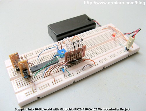
But for showing the basic PIC24F16KA102 microcontroller peripheral features in this tutorial, we could easily prototype it on the breadboard.

Ok now let list down the necessary electronics components and supported software for our stepping into 16-bit world tutorial and make sure you have the Microchip PIC24F16KA102 microcontroller datasheet near you:
1. Resistors: 330 Ohm (9), 470 Ohm (1) and 10K (2)
2. Capacitors: 0.01uF (2) and 0.1uF (2)
3. LEDS: 3 mm Blue LED (8) and 3 mm Red LED (1)
4. One Microchip 16-bit PIC24F16KA102 microcontroller
5. Two momentary push button
6. One Breadboard and some breadboard’s jumper cables
7. One 2xAA Battery Holder with the 2x AA Alkaline battery (3 volt) for powering the circuit
8. Microchip PICKit3 programmer (used in this project)
9. Microchip MPLAB IDE version 8.47 and Microchip C30 Compiler version 3.30
10. Microchip PIC24 Reference Document: PIC24F16KA102/101 datasheet, AN39703a (CPU), AN39711b (I/O), AN39704a (Timer), AN39705b (ADC)

For quick prototyping this project on the breadboard I used the SIL LED display and SIL push button modules which you could read more about it in my previous posted blog Single In Line (SIL) LED Display for your Microcontroller Project

The 16-bit PIC24 Family Microcontroller
With 16-bit CPU internal data path, the PIC24 family microcontroller is being referred as the 16-bit class microcontroller. This means this microcontroller could process the 16-bit or 8-bit data with just a single instruction. As the result compared to the 8-bit class microcontroller the 16-bit class microcontroller will perform better for intensive arithmetic calculation application such as GUI (graphics user interface) display, TCP/IP application, USB embedded host and digital signal controlling (dsPIC microcontroller family).
Unlike the Microchip 8-bit (PIC12, PIC16 and PIC18) families microcontroller, the Microchip 16-bit PIC24 microcontroller families has a linear memory addressing design, therefore we don’t have to switch back and forth between memory “BANK” to access different peripheral registers as we do in the Microchip 8-bit families microcontroller; you could read more about programming the Microchip 8-bit microcontroller on my previous posted blog Introduction to Microchip PIC Assembler Language – Part 1.

The 16-bit Microchip PIC microcontroller also has 16 x 16-bit array working register known as W0 through W15 compared to only one working register in Microchip PIC 8-bit (WREG), this make the programming code is more efficient comparing to the PIC 8-bit microcontroller because all the arithmetic operation should go through the working register in order to be processed. The Microchip PIC24 microcontroller class also only use 2 cycles clock per instruction compared to 4 cycles clock per instruction on the PIC12/16/18 microcontroller class; this make the PIC24 at least twice more faster than PIC12/16/18 microcontroller. And the best of all, we still use the same Microchip powerful MPLAB integrated development environment for debugging, compiling and programming this 16-bit class microcontroller.
For more detail information about the Microchip 16-bit microcontroller families, I suggest to read more about it in the Microchip 16-bit microcontroller home website. Ok let’s start with the hello 16-bit world C program, where we simply blink one LED using the PIC24F16KA102 microcontroller output port as shown on this following C code:
/* ***************************************************************************
**  File Name    : helloworld.c
**  Version      : 1.0
**  Description  : First 16-bit PIC C Programming
**  Author       : RWB
**  Target       : PIC24F16KA102
**  Compiler     : MPLAB C30 C Compiler v3.23
**  IDE          : Microchip MPLAB IDE v8.46
**  Programmer   : PICKit3 (Firmware Suite Version 01.25.20)
**  Last Updated : 08 April 2010
** ***************************************************************************/
#include <p24fxxxx.h>
// PIC24F16KA102 Configuration bits
/*
** --------------------------------------------------------------------
** _FBS (Register FBS: 0xF80000)
**  BWRP_OFF - Boot Segment Write Protect Disable
**  BSS_OFF  - Boot Segment Code Protect Disable
** --------------------------------------------------------------------
** _FGS (Register FGS: 0xF80004)
**  GWRP_OFF - General Segment Write Protect Disable
**  GCP_OFF  - General Segment Code Protect Disable
** --------------------------------------------------------------------
** _FOSCSEL (Register FOSCSEL: 0xF80006)
**  FNOSC_FRCDIV - Fast RC Oscillator With Postscale (FRCDIV)
**  IESO_OFF - Two Speed Start-up Disable
** --------------------------------------------------------------------
** _FOSC (Register FOSC: 0xF80008)
**  FCKSM_CSECMD - Clock Switching Enabled, Clock Monitor Disabled
**  POSCFREQ_MS  - Mid Speed (100kHz - 8MHz)
**  OSCIOFNC_ON  - OSCO Pin Has Digital I/O Function (RA3)
**  POSCMOD_NONE - Primary disabled
**  SOSCSEL_SOSCLP - Low Power Secondary Oscillator
** --------------------------------------------------------------------
** _FWDT (Register FWDT (0xF8000A)
**  FWDTEN_OFF - Watchdog Timer (WDT) Disable
**  WINDIS_OFF - Non-Window WDT Mode
**  FWPSA_PR128 - WDT Prescale 1:128
**  WDTPS_PS32768 - WDT Postscale 1:32,768
** --------------------------------------------------------------------
** _FPOR (Register FPOR: 0xF8000C)
**  MCLRE_OFF - MCLR Disabled, RA5 Enabled
**  BORV_LPBOR - Low Power BOR (Brown Out Voltage)
**  BOREN_BOR3 - Enabled in hardware, SBOREN bit disabled
**  I2C1SEL_PRI - Use SCL1/SDA1 Pins For I2C1
**  PWRTEN_OFF - Power Up Timer Disabled
** --------------------------------------------------------------------
** _FICD (Register FICD: 0xF8000E)
**  BKBUG_OFF - Background Debugger Disabled
**  ICS_PGx3 - EMUC/EMUD share PGC3/PGD3
** --------------------------------------------------------------------
** _FDS (Register FDS: 0xF80010)
**  DSWDTEN_OFF - Deep Sleep WDT Disabled
**  DSBOREN_ON - Deep Sleep BOR Enabled
**  RTCOSC_SOSC - RTCC Oscillator select: Secondary Oscillator (SOSC)
**  DSWDTOSC_SOSC - Deep Sleep WDT Low Power RC Oscillator (LPRC)
**  DSWDTPS_DSWDTPSF - Deep Sleep WDT Postscale 1:2,147,483,648
**                     (25.7 Days)
** --------------------------------------------------------------------
*/
_FBS(BWRP_OFF & BSS_OFF)
_FGS(GWRP_OFF & GCP_OFF)
_FOSCSEL(FNOSC_FRCDIV & IESO_OFF)
_FOSC(FCKSM_CSECMD & POSCFREQ_MS & OSCIOFNC_ON & POSCMOD_NONE & SOSCSEL_SOSCLP)
_FWDT(FWDTEN_OFF & WINDIS_OFF & FWPSA_PR128 & WDTPS_PS32768)
_FPOR(MCLRE_ON & BORV_LPBOR & BOREN_BOR3 & I2C1SEL_PRI & PWRTEN_OFF)
_FICD(BKBUG_OFF & ICS_PGx3)
_FDS(DSWDTEN_OFF & DSBOREN_ON & RTCOSC_SOSC & DSWDTOSC_SOSC & DSWDTPS_DSWDTPSF)
int main ( void )
{
  unsigned int i;

  // Use Internal 8 MHz Clock
  OSCCON = 0x0000;
  CLKDIV = 0x0000;
  // Initial the Ports Used
  TRISB  = 0xFF00;         // Set all RB0-RB7 Output, RB8-RB15 Input
  AD1PCFG = 0xffff;        // Set all to digital output
  ODCB   = 0x0000;         // Do not use open drain Output
  LATB   = 0x0000;         // Reset All PORT B
  for(;;) {
    PORTBbits.RB0=1;           // Turn On RB0
    for (i=0; i<0xffff; i++);  // Delay Loop
    PORTBbits.RB0=0;           // Turn Off RB0
    for (i=0; i<0xffff; i++);  // Delay Loop
  }
  return 0;
}
/* EOF: helloworld.c */
The PIC24F16KA102 Output Port
One of the advantages using the PIC2F16KA102 microcontroller is each of the output ports could be configured as the open drain output using the Open Drain Control Register (e.g. ODCB). By setting this 16-bit register to logical “1” we could configure the port as the open drain output where the P-channel MOSFET transistor is disconnect from the microcontroller output port and leave the N-Channel MOSFET transistor with the open drain (not connected to Vcc). In order for the open drain output to work you need to supply the Pull-up resistor to power the N-Channel MOSFET transistor. Remember when you configure as the open drain output, the output port only could sink current through the N-Channel MOSFET transistor.

The advantages of open drain output feature is, it has a very nice application in terms of making the microcontroller electronics support circuit design simpler such as wire ORing and it could be used as the logical voltage shifter to interface from 3.3 volt logic circuit to 5 volt circuit as shown on this following picture:

Before using the PIC24F16KA102 microcontroller I/O port, first we have to set whether to use it as input or output port by setting the tri state register for PORTB (i.e. TRISB) as follow:
// Initial the Ports Used
TRISB  = 0xFF00;         // Set all RB0-RB7 Output, RB8-RB15 Input
AD1PCFG = 0xffff;        // Set all to digital output
ODCB   = 0x0000;         // Do not use open drain Output
LATB   = 0x0000;         // Reset All PORT B
By setting the TRISB register bits (TRISB1 to TRISB15) to logical “1” we define the port as input (you could see it as “I” for input) and by setting it to logical “0” we define the port as output (you could see it as “O” for output), therefore by setting the TRISB register bits to 0xFF00, mean we set the RB0 to RB7 as output ports while the RB8 to RB15 as the input ports.
Next we configure the ADC (analog to digital conversion) pin configuration register AD1PCFG bits to logical “0“, this mean we configure all of the 10 ADC channel port available in PIC24F16KA102 microcontroller as the digital I/O port. By setting the ODCB register bits to logical “0” we disable the output port open drain feature which we need it in this project to drive the display LED. The last is we simply set the PORTB latch register (LATB) to reset all the display LED. Writing to the PORTB latch register (LATB) will give the same result as we write directly to the PORTB register.
Using the TIMER Peripheral for Generating Delay
From the above example you’ve noticed that I used simply loops to create delay for displaying the LED; the more elegant way to make the delay is to take advantage of the PIC24F16KA102 microcontroller TIMER peripherals. To show how the TIMER peripheral work I modified the above code and add the capabilities to read input from SW2 as well as using the TIMER1 peripheral as the base of our delay routine. Now let’s examine the following C code (ledseq.c):
/* ***************************************************************************
**  File Name    : ledseq.c
**  Version      : 1.0
**  Description  : LED Sequence 16-bit PIC C Programming
**  Author       : RWB
**  Target       : PIC24F16KA102
**  Compiler     : MPLAB C30 C Compiler v3.23
**  IDE          : Microchip MPLAB IDE v8.46
**  Programmer   : PICKit3 (Firmware Suite Version 01.25.20)
**  Last Updated : 08 April 2010
** ***************************************************************************/
#include <p24fxxxx.h>
// PIC24F16KA102 Configuration bits
_FBS(BWRP_OFF & BSS_OFF)
_FGS(GWRP_OFF & GCP_OFF)
_FOSCSEL(FNOSC_FRCDIV & IESO_OFF)
_FOSC(FCKSM_CSECMD & POSCFREQ_MS & OSCIOFNC_ON & POSCMOD_NONE & SOSCSEL_SOSCLP)
_FWDT(FWDTEN_OFF & WINDIS_OFF & FWPSA_PR128 & WDTPS_PS32768)
_FPOR(MCLRE_ON & BORV_LPBOR & BOREN_BOR3 & I2C1SEL_PRI & PWRTEN_OFF)
_FICD(BKBUG_OFF & ICS_PGx3)
_FDS(DSWDTEN_OFF & DSBOREN_ON & RTCOSC_SOSC & DSWDTOSC_SOSC & DSWDTPS_DSWDTPSF)
void delay_ms(unsigned short ms)
{
  unsigned short i;
  // TIMER1 Period = PR1 x 2 x Tosc x Prescale second
  // TIMER1 Period = 500 x 2 x 1/8000000 x 8 = 0.001 second = 1 ms

  PR1=500;                      // Maximum Counter
  for (i=0; i < ms;i++) {
    TMR1=0;                     // Reset TIMER1 Counter
    IFS0bits.T1IF=0;            // Clear TIMER1 Interrupt Flag
    T1CONbits.TON=1;            // Turn On TIMER1
    while(IFS0bits.T1IF != 1);  // Wait until TMR1 > PR1 (Overflow)
    T1CONbits.TON=0;            // Turn Off TIMER1
  }
}
int main ( void )
{
  unsigned char mode,count,led_pointer;
  char led_pattern0[10]= {0b00000011,0b00001100,0b00110000,0b11000000,0b00000000,
                          0b11000000,0b00110000,0b00001100,0b00000011,0b00000000};
  char led_pattern1[10]= {0b00000001,0b00000100,0b00010000,0b01000000,0b00000000,
                          0b10000000,0b00100000,0b00001000,0b00000010,0b00000000};

  // Use Internal 8 Mhz Clock
  OSCCON = 0x0000;
  CLKDIV = 0x0000;
  // Initial the Ports Used
  TRISB  = 0xFF00;         // Set all RB0-RB7 Output, RB8-RB15 Input
  CNPU1bits.CN11PUE = 0;   // Disable Week Pull Up on RB15/CN11 Input
  AD1PCFG = 0xFFFF;        // Set all to digital I/O
  ODCB   = 0x0000;         // Do not use open drain Output
  LATB   = 0x0000;         // Reset All PORT B
  // Initial TIMER1 for Delay
  T1CON=0x0010;            // TIMER1 Off, Prescale 1:8 using the internal clock
  // Initial Variables Used
  mode=0;
  count=0;
  led_pointer=0;
  for(;;) {
    // Reading the Switch Input on RB15
    if (PORTBbits.RB15 == 0) {
      if (count++ > 5) {   // The Debouce Count
        count=0;
        mode=~mode;        // Toggle the mode variable
      }
    }

    // Display the LED Pattern
    if (mode)
      PORTB=led_pattern1[led_pointer];
    else
      PORTB=led_pattern0[led_pointer];

    if (led_pointer++ > 9)
      led_pointer=0;
    delay_ms(50);          // Call Delay Function
  }
  return 0;
}
/* EOF: ledseq.c */
The Microchip PIC24F16KA102 microcontroller have build in three independent 16-bit TIMER (TIMER1, TIMER2 and TIMER3) where TIMER2 and TIMER3 could be configured as a single 32-bit TIMER. On this tutorial we will use the 16-bit TIMER1 as our delay routine base.
As implied by its name, you could look the TIMER1 as an ordinary 16-bit counter named TMR1; where you could use the external or internal clock to pulse this counter controlled by the TIMER1 control register (T1CON). As the counter value is incremented by the pulse, the 16-bit counter output is constantly compared to the PR1 register when TMR1 reach the PR1 value than the the TIMER1 will automatically set the TIMER1 interrupt flag (T1IF) bit on Intterupt Flag Status 0 register (IFS0).

By using the correct TIMER1 clock prescale and PR1 value we could calculate the TIMER1 period using this following formula:
TIMER1 Period = PR1 x 2 x Tosc x Prescale
By assigning the PR1 register to 500, using 8 MHz internal system clock and with 1:8 prescale than the TIMER1 period could be calculated as follow:
TIMER1 Period = 500 x 2 x 1/8000000 x 8 = 0.001 second = 1 ms
Therefore by waiting for the T1IF bit to become logical “1” by the TIMER1 comparator inside the loop, we could create configurable delay function base on the TIMER1 as show on this following C code:
....
PR1=500;                      // Maximum Counter
for (i=0; i < ms;i++) {
  TMR1=0;                     // Reset TIMER1 Counter
  IFS0bits.T1IF=0;            // Clear TIMER1 Interrupt Flag
  T1CONbits.TON=1;            // Turn On TIMER1
  while(IFS0bits.T1IF != 1);  // Wait until TMR1 > PR1 (Overflow)
  T1CONbits.TON=0;            // Turn Off TIMER1
}
Reading the Input Port
Reading the input port is done by first configured the I/O port as the input port. When we configure as the input port in the PIC24F16KA102 microcontroller, you could activate the weak pull-up resistor as shown on this following picture:

To enable or disable the weak pull-up resistor we could set the CNxPUE corresponding bits to either “1” (enable) or “0” (disable) in the PIC24F16KA102 microcontroller pull-up control register CNPU1 or CNPU2. In this tutorial because we use the external pull-up resistor, therefore we disable this feature.
TRISB  = 0xFF00;         // Set all RB0-RB7 Output, RB8-RB15 Input
CNPU1bits.CN11PUE = 0;   // Disable Week Pull Up on RB15/CN11 Input
Now by reading the switch on RB15 on PORTB and using simple debounce logic we could easily read the switch input status whether it being pressed or not. This status later on will toggle the mode variable to control how we display the LED pattern data on the PORTB output as shown on this following C code:
// Reading the Switch Input on RB15
if (PORTBbits.RB15 == 0) {
  if (count++ > 5) {   // The Debounce Count
    count=0;
    mode=~mode;        // Toggle the mode variable
  }
}
Using the ADC (Analog to Digital Converter) Peripheral
On the last of this introduction to 16-bit world tutorial, I’m going to explain one of the most important peripheral features on every modern microcontroller which is the Analog to Digital Conversion (ADC) peripheral. Again by slightly modify the example code above I added the capability to adjust the speed of the LED display pattern by using the trimport. Now let’s take a look on this following C code (adcled.c):
* ***************************************************************************
**  File Name    : adcled.c
**  Version      : 1.0
**  Description  : ADC LED Sequence 16-bit PIC C Programming
**  Author       : RWB
**  Target       : PIC24F16KA102
**  Compiler     : MPLAB C30 C Compiler v3.23
**  IDE          : Microchip MPLAB IDE v8.46
**  Programmer   : PICKit3 (Firmware Suite Version 01.25.20)
**  Last Updated : 10 April 2010
** ***************************************************************************/
#include <p24fxxxx.h>
// PIC24F16KA102 Configuration bits
_FBS(BWRP_OFF & BSS_OFF)
_FGS(GWRP_OFF & GCP_OFF)
_FOSCSEL(FNOSC_FRCDIV & IESO_OFF)
_FOSC(FCKSM_CSECMD & POSCFREQ_MS & OSCIOFNC_ON & POSCMOD_NONE & SOSCSEL_SOSCLP)
_FWDT(FWDTEN_OFF & WINDIS_OFF & FWPSA_PR128 & WDTPS_PS32768)
_FPOR(MCLRE_ON & BORV_LPBOR & BOREN_BOR3 & I2C1SEL_PRI & PWRTEN_OFF)
_FICD(BKBUG_OFF & ICS_PGx3)
_FDS(DSWDTEN_OFF & DSBOREN_ON & RTCOSC_SOSC & DSWDTOSC_SOSC & DSWDTPS_DSWDTPSF)
void delay_ms(unsigned short ms)
{
  unsigned short i;
  // TIMER1 Period = PR1 x 2 x Tosc x Prescale second
  // TIMER1 Period = 500 x 2 x 1/8000000 x 8 = 0.001 second = 1 ms

  PR1=500;                      // Maximum Counter
  for (i=0; i < ms;i++) {
    TMR1=0;                     // Reset TIMER1 Counter
    IFS0bits.T1IF=0;            // Clear TIMER1 Interrupt Flag
    T1CONbits.TON=1;            // Turn On TIMER1
    while(IFS0bits.T1IF != 1);  // Wait until TMR1 > PR1 (Overflow)
    T1CONbits.TON=0;            // Turn Off TIMER1
  }
}
int main ( void )
{
  unsigned char mode,count,led_pointer;
  char led_pattern0[10]= {0b00000011,0b00001100,0b00110000,0b11000000,0b00000000,
                          0b11000000,0b00110000,0b00001100,0b00000011,0b00000000};
  char led_pattern1[10]= {0b00000001,0b00000100,0b00010000,0b01000000,0b00000000,
                          0b10000000,0b00100000,0b00001000,0b00000010,0b00000000};
  unsigned int iDelay;

  // Use Internal 8 Mhz Clock
  OSCCON = 0x0000;
  CLKDIV = 0x0000;
  // Initial the Ports Used
  TRISB  = 0xFF00;         // Set all RB0-RB7 Output, RB8-RB15 Input
  CNPU1bits.CN11PUE = 0;   // Disable Week Pull Up on RB15/CN11 Input
  AD1PCFG = 0xFFFF;        // Set all to digital I/O
  ODCB   = 0x0000;         // Do not use open drain Output
  LATB   = 0x0000;         // Reset All PORT B
  // Initial TIMER1 for Delay
  T1CON=0x0010;            // TIMER1 Off, Prescale 1:8
  // Initial the ADC Peripheral
  AD1PCFGbits.PCFG12 = 0;  // Set AN10/RB12 as Analog Input
  AD1CON1 = 0x00E0;        // Auto convert after end of sampling
  AD1CON2 = 0x0000;        // Use MUXA, Internal AVdd and AVss as reference, 16-word buffer
  AD1CON3 = 0x1F02;        // Use System clock and Max sample time = 31 TAD, TAD = 3 Tcy
  AD1CSSL = 0x0000;        // No inputs are scanned
  AD1CON1bits.ADON=1;      // Turn ON ADC Peripheral
  // Initial Variables Used
  mode=0;
  count=0;
  led_pointer=0;
  iDelay=50;
  for(;;) {
    // Reading the Switch Input on RB15
    if (PORTBbits.RB15 == 0) {
      if (count++ > 5) {       // The Debounce Count
        count=0;
        mode=~mode;            // Toggle the mode variable
      }
    }
    // Start ADC Conversion
    AD1CHS = 0x000C;               // Read Trimport on Channel 12 (AN12)
    AD1CON1bits.SAMP=1;            // Now Start the ADC Sampling
    while (AD1CON1bits.DONE != 1); // Wait for ADC conversion
    iDelay=ADC1BUF0;               // Get the 10-bit ADC Result

    // Display the LED Pattern
    if (mode)
      PORTB=led_pattern1[led_pointer];
    else
      PORTB=led_pattern0[led_pointer];

    if (led_pointer++ > 9)
      led_pointer=0;
    delay_ms(iDelay);          // Call Delay Function
  }
  return 0;
}
/* EOF: adcled.c */
Differ from the 8-bit PIC12/16/18 microcontroller families, the 16-bit PIC24 microcontroller ADC peripheral support many advance features such as two independent multiplexing analog channels, multiple single channel A/D conversion or multiple multi channel A/D conversion for single interrupt, four type of A/D conversion data format result (integer, signed integer, fractional and signed fractional) and multiple trigger A/D data conversion method.
The PIC24 families A/D conversion required one A/D clock cycle (TAD) plus 2 additional clock cycles, thus the PIC24 SAR need at least 12 TAD cycles to do the 10-bit conversion. For correct A/D conversions, the A/D conversion clock (TAD) must be selected to ensure a minimum TAD time of 75 ns.

Finally when the conversion is done, the result is loaded into the sixteen words of A/D result buffer array registers (ADC1BUF0 to ADC1BUFF). On this tutorial I used one channel (AN12) with manual sample start A/D conversion method.

The ADC peripheral initialization begin by setting the input pin AN12 (RB12) to be functioned as the analog input by setting PCFG12 bit to logical “1” on ADC pin configuration register (AD1PCFG). Then we continue to ADC peripheral control registers AD1CON1, AD1CON2 and AD1CON3 as shown on this following C code:
// Initial the ADC Peripheral
AD1PCFGbits.PCFG12 = 0;  // Set AN10/RB12 as Analog Input
AD1CON1 = 0x00E0;        // Auto convert after end of sampling
AD1CON2 = 0x0000;        // Use MUXA, Internal AVdd and AVss as reference, 16-word buffer
AD1CON3 = 0x1F02;        // Use internal RC clock and Max sample time = 31 TAD, TAD = 3 Tcy
AD1CSSL = 0x0000;        // No inputs are scanned
AD1CON1bits.ADON=1;      // Turn ON ADC Peripheral

Because in this tutorial I used automatic A/D conversion after the sample and hold amplifier captured the analog signal input, therefore we have to set the A/D conversion source trigger bits (SSRC<2:0>) on AD1CON1 register to “111” to use internal counter for automatic conversion after sampling and set the ASAM bits to logical “0” to instruct the sample and hold amplifier to begin the sampling when the SAMP bit on register AD1CON1 is set to logical “1“.
Next on the AD1CON2 register we choose the PIC24K16KA102 power supply as our A/D reference voltage by setting the voltage configuration bits (VCFG<2:0>) to “000” and configure the A/D result buffer as single word (16-bit) by setting the buffer mode bit (BUFM) to logical “0“. Finally on the AD1CON3 register we configure the A/D conversion clock, because we need at least 75 ns for A/D conversion time (TAD), therefore by setting the conversion period selection bits (ADCS<7:0>) to “00000010” (ADCS = 2) we could calculate the TAD for 8MHz internal clock source (FOSC) as follow:
TAD = (ADCS + 1) x TCY
Because the instruction cycle clock is FOSC/2, therefore the instruction cycle period (TCY) will be 2/FOSC
TAD = 3 x 1 / 8000000 x 2 = 750 ns
Before starting the A/D conversion we have to turn on the ADC peripheral by setting the ADON bit on register AD1CON1 to logical “1” then next selecting the analog input channel using the A/D channel selection register (AD1CHS) to AN12 pin (0x000C):
...
// Start ADC Conversion
AD1CHS = 0x000C;               // Read Trimport on Channel 12 (AN12)
AD1CON1bits.SAMP=1;            // Now Start the ADC Sampling
while (AD1CON1bits.DONE != 1); // Wait for ADC conversion
iDelay=ADC1BUF0;               // Get the 10-bit ADC Result
...
After starting the sample and hold amplifier for sampling the analog input, the ADC peripheral will automatically do the conversion after 31 TAD and by examining the DONE bit on the AD1CON register we could get the A/D conversion status and later read the A/D conversion result on the ADC1BUF0 register. This A/D conversion result than will be used as the delay parameter for displaying the LED, therefore by adjusting the 10K trimport we could adjust the LED display speed.

After compiling and downloading all the HEX code into the PIC24F16KA102 microcontroller you will have similar result as shown on this following video:
The Final Thought
As you walk through this 16-bit microcontroller world tutorial you will noticed that although the inside architecture between the 8-bit (Harvard) and 16-bit (Modified Harvard) Microchip PIC microcontroller is different, but they shared the same designed pattern such as the peripheral register name, the pins name and they all use the Microchip MPLAB integrated development environment. This make move from the 8-bit to the 16-bit class microcontroller become straightforward and easy. By using the 16-bit class microcontroller, you could bring broader range of application into the embedded world.
Bookmarks and Share


Related Posts
4 Responses to “Stepping Into the 16-bit World with the Microchip 16-bit PIC24F16KA102 Family Microcontroller”
Comment by rwb.
Its better to compile the code with newest release of MPLAB IDE from Microchip
Comment by jalpa.
Hi,
i am using microstick as an hardware for the PIC24f16KA102 and i m using MPLABX IDE when i use the code of blog as it is for timer to generate pulse it is remaining continuously on. I have pasted code here. thanks
Comment by rwb.
Make sure you correctly install the latest MPLAB IDE and you have a similar hardware circuit as shown on the project.

Comment by nguyencong.
you can send file hex.tks