Blog Entry
Introduction to Microchip PIC Assembler Language – Part 2
April 21, 2009 by rwb, under Microcontroller.
With only 35 instructions to learn the Microchip PIC microcontroller assembler language is considered very efficient and easy to learn; you will not find such as Atmel AVR microcontroller CP (compare) and BRNE (branch if not equal) or BRGE (branch if greater or equal) on the PIC microcontroller assembler language dialect, instead it’s just provide us with a very simple bit test and skip one line instruction. This fact is what makes programming the PIC microcontroller assembler language become very interesting and challenging, therefore although is easy to learn but for sure you will need a lot of flying time in order to code the PIC microcontroller efficiently.
The PIC Assembler Program Skeleton:
Continuing our lesson with the 8-bit, 8 pins midrange Microchip PIC12F683 microcontroller, I will start with the typical PIC microcontroller assembler program skeleton bellow:

The first part is the program comment; it’s always a good practice to put a comment to your program e.g. name, version, description, etc. All lines begin with ; sign is consider a comment to the MPASM (Microchip PIC Assembler) compiler.
The second part is the #include <p12F683.INC> MPASM compiler directive which tell the compiler to include the PIC12F683.INC file definition which exist in the c:\Program Files\Microchip\MPASM Suite directory (MPLAB IDE v8.00 default installation). This include file contain the standard PIC microcontroller physical address to the equivalent naming convention; for example instead of using the address 0x05 (5 hex) for general purpose I/O, we could use GPIO which is easier to remember.
The third part is the Microchip PIC microcontroller configuration bits register; this register is start at address 2007 on the PIC12F683 microcontroller and has 14 bits long. This register is one of the unique features of the PIC Microcontroller compared to other microcontroller, the PIC configuration bits could be configured on every startup of the program.
The configuration bits register is used to set how the PIC microcontroller work such as choosing the internal or external clock, using the master clear or not, etc. When programmed these bits will be read as “0“; for un-programmed these bits will be read as “1“. The following table shows the configuration bit used in our Hello World assembler program.

The complete description of this configuration bit could be found at page 84 on the Microchip PIC12F63 microcontroller datasheet; therefore by using the AND operator to the entire PIC MPASM configuration bit definition value we could configure the desire configuration bit register value or we could simply using just the bit value as shown on this following table:

Base on the configuration bit table shown above, we could set the PIC12F683 microcontroller configuration bit directly and this will give you the same result as the above program example:
__config 0x33D4
The fourth part is the MPASM CBLOK 0x20 and closed with ENDC directive; which tell the MPASM compiler to map the Delay1 and Delay2 variables to the 8-bit general purpose registers which start at the address 0x20 on the PIC12F683 microcontroller address BANK 0; the Delay1 will be mapped to the general purpose register at the address 0x20 and the Delay2 will be mapped to the general purpose register at the address 0x21. The following picture show all the Microchip PIC12F683 microcontroller registers address which split into 2 groups named BANK 0 and BANK 1.

One of the unique things about the PIC microcontroller registers address comparing to other microcontroller that the address is not in one continues memory but its being split into two BANKS (groups); this mean we have to switch back and forth between the BANK addresses to access the desire register. For example if we want to access the register TRISIO, we have to switch to the BANK 1 before we could access it and switch back to the BANK 0 in order to access the GPIO register.
To make it easier to understand you could consider the BANK 0 and BANK 1 are like the DIRECTORIES in your computer file system, so if you want to access the TRISIO register (just like a file reside in your directory), you have to change the directory first to the BANK 1 before you could use this register and change directory back to the BANK 0 to access the GPIO register. If you notice some of the registers such as the STATUS register is shared or appeared to the both BANKS; this mean it doesn’t matter which BANK you are right now, you could always access this register. This is the same principal as the LINK file on the UNIX/Linux operating system file system, that one physical file could appear on many directories using just the link name.
The fifth part is the ORIGINATE (org) MPASM compiler directive that tell the MPASM compiler that your code is start at the address 0x0000 of the PIC microcontroller flash memory.
The sixth part is where you put your PIC assembler program code; this code could consist of main program and the subroutine or function.
The last part is the end MPASM compiler directive that tell the MPASM compiler that your code is end here and it’s a good practice to put the EOF (end of file) comment mark in your program so whenever you cut and paste the program to the other project you could make sure that all the codes is being copied until the EOF mark.
Inside the HelloWorld Program
Now we will walk through the program codes, first thing I will explain the initialization routine to the PIC12F683 microcontroller; in this initialization routine you will learn the top five of the 35 PIC12F683 microcontroller assembler instructions that you will certainly use in every project. Before we start make sure you have the PIC12F683 datasheet near you and open the page 101 on the Instruction Set Summary.
Start:
     bsf    STATUS,RP0    ; Select Registers at Bank 1
     movlw  0x70
     movwf  OSCCON        ; Set the internal clock speed to 8 Mhz
     clrf   TRISIO        ; Set all General Purpose I/O to output
     clrf   ANSEL         ; Make all ports as digital I/O
     bcf    STATUS,RP0    ; Back to Registers at Bank 0
The first thing in our initialization routine is to set the internal clock speed which can be controlled in the oscillator control register or OSCCON at BANK 1, we decide to run the PIC12F683 microcontroller with the maximum internal clock speed of 8 Mhz as shown on the OSCCON register bellow:

By making the internal oscillator selection bits IRCF2=1, IRCF1=1 and IRCF0=1 on the OSCCON register we select the 8 Mhz of internal oscillator frequency, this could be written as the following C program:
OSCCON = 0x70;
But in the PIC assembler code, before we could use the OSCCON register we have to change to the BANK 1, since the default BANK when the PIC microcontroller power up is in the BANK 0; How to instruct the PIC microcontroller to change to the BANK 1; this could be done by setting the bank selection register bits RP1 and RP0 on the STATUS register.

Because the PIC12F683 microcontroller only have two BANKS, then the RP1 bit is not use; but for some PIC microcontroller families such as PIC16F690 or PIC16F886 families have four BANK addresses; therefore for this PIC microcontroller families both RP1 and RP0 bits are used to select the BANK addresses. By setting the bit RP0 to logical “1” we instruct the PIC12F683 microcontroller to change to the BANK 1 and by clearing the bit RPO to logical “0“, we instruct the PIC12F683 microcontroller to change back to the BANK 0 (default). The famous PIC set and clear bit oriented file register operation could be used to achieve this task.
bsf f,b -> Bit Set f: Register Address (0x00 to 0x7F) and b: is the bit address
bcf f,b -> Bit Clear f: Register Address (0x00 to 0x7F) and b: is the bit address
bsf STATUS,RP0 ; Select Registers at Bank 1
This instruction will simply tell the PIC microcontroller to SET the RPO bit (the fifth bit) on the STATUS (address 0x03) register and to CLEAR the RPO bit on the STATUS register we use this command bellow:
bcf STATUS,RP0 ; Back to Registers at Bank 0
As you seen from time to time we have to change the BANK address in order to access the desired registers and we always use the STATUS register to achieve this task; therefore now you understand why the PIC microcontroller shared this STATUS register through all the PIC’s BANK addresses, so you could always access this important register regardless of the BANK address you are in right now.
After we change to the BANK 1 in order to assign the 0x70 value into the OSCCON register, we have to put first the value in the PIC microcontroller 8-bit accumulator register named WREG (working register) and then move this accumulator value into the OSCCON register. Again the two most used PIC assembler instructions will be used to achieve these tasks:
movlw k -> Move literal (constant) to WREG, k is the 8-bit constant
movwf f -> Move the WREG value to f: Register Address (0x00 to 0x7F)
movlw  0x70
movwf  OSCCON        ; Set the internal clock speed to 8 Mhz
The tri-state register TRISIO and the analog selection register ANSEL located at BANK 1 are used to set the PIC microcontroller I/O port behavior:

By setting all these bits on the TRISIO register to logical “0“, we instruct the PIC12F683 microcontroller to set all of the general purpose I/O (GPIO) as the OUTPUT port.

Again by setting all these bits on the ANSEL register to logical “0“, we instruct the PIC12F683 microcontroller to use all the analog ports on the PIC12F683 general purpose I/O (GPIO) as the digital port I/O. The PIC assembler instruction to achieve these tasks is by using the byte oriented file register operation bellow:
clrf f -> Clear Register f: Register Address (0x00 to 0x7F)
clrf   TRISIO        ; Set all General Purpose I/O to output
clrf   ANSEL         ; Make all ports as digital I/O
The last thing to be explained on the initialization routine is the Start: label, this label is used just to clarify that this is beginning of the code; all the labels appear in the codes automatically will be converted to the corresponding program address by the MPASM compiler when we use it such as in the loop and branch instruction.
The Infinite Loop
After the initialization routine we enter to the infinite loop routine, inside the infinite loop we will turn on the LED attached to the general purpose I/O GP2 do some delay and turn off the LED and do some delay again. In this infinite loop codes we will learn three more PIC assembler instruction beside the two clear bit oriented file register operation instructions you’ve just learned; to turn on and off the LED.
MainLoop:
     bsf    GPIO,2        ; Set GP2 Output To High
     call   Delay         ; Call Delay Subroutine
     bcf    GPIO,2        ; Clear GP2 Output To Low
     call   Delay         ; Call Delay Subroutine
     nop                  ; No Operation
     goto   MainLoop      ; Goto MainLoop
The main function of the infinite loop codes is to turn on and off the LED by setting GP2 bit (2) on the GPIO register to logical “1” and to logical “0“.

Therefore by using the bsf and bcf instruction we could simply turn on and off the LED attached to the GP2 port on the GPIO register.
bsf    GPIO,2        ; Set GP2 Output To High
bcf    GPIO,2        ; Clear GP2 Output To Low
Intentionally I put the number 2 instead of GP2, just to remain you that the GP2 bit definition actually is defined as 2 in the P12F683.INC include file mentioned above and also the GPIO register definition. This will become clear when you look at the disassembly code listing on the MPLAB IDE v8.0 (menu View -> Disassembly Listing); you will not get the GP2 or GPIO words, instead you will get their original value as follow:
bsf    0x05,0x2       ; Set GP2 Output To High
bcf    0x05,0x2       ; Clear GP2 Output To Low

The call and goto instructions are simply tell the PIC microcontroller to jump to the label (program address) and start executes the code from there. The call instruction is used to call the subroutine and when the PIC microcontroller execute this instruction it will save the next instruction program address to the hardware stack and then jump to called program address and when it encounter the return instruction it will retrieve back the program address stored in the hardware stack and put it on the program counter register so the PIC microcontroller could start execute from there.

The PIC12F683 microcontroller has 8 hardware stacks; this mean the maximum call’s deep levels are 8. The last instruction inside the infinite loop is the nop (no operation) instruction; this instruction will do nothing, usually is used to put a single instruction delay to the code or simply as the break point to examine the registers content for debugging purpose.
The Delay Subroutine
In order to be able to watch the on/off LED operation on GP2 port, we have to put the delay subroutine. In this delay subroutine you will learn two more PIC microcontroller assembler instruction. The following is the Delay subroutine code used in the program:
Delay:
     movlw  0xFF
     movwf  Delay2
DelayLoop1:
     movlw  0xFF
     movwf  Delay1
DelayLoop2:
     decfsz Delay1,f      ; Decrease Delay1, If zero skip the next instruction
     goto   DelayLoop2    ; Not zero goto DelayLoop2
     decfsz Delay2,f      ; Decrease Delay2, If zero skip the next instruction
     goto   DelayLoop1    ; Not zero goto DelayLoop1
     return               ; Return to the Caller
The first new instruction is the decfsz which mean decrease the register f, if the register value is zero than skip one instruction:
decfsz f,d -> Decreament f: Register Address (0x00 to 0x7F) , d: Destination -> w: WREG or f: register
If we select the WREG destination (w) than the decrement result value will be put on the WREG (working register) register, if the destination is the register (f) than the result is not passed to the WREG register. Therefore by decreasing the value of general purpose register 0x21 (Delay1) we could create a simple delay as follow:
DelayLoop2:
     decfsz Delay1,f      ; Decrease Delay1, If zero skip the next instruction
     goto   DelayLoop2    ; Not zero goto DelayLoop2
By using the two loops we could achieve the longer delay. As you see from the PIC assembler code above, the equivalent C code for the delay routine could be written as the following code:
unsigned char Delay1, Delay2;
Delay2=0xff;
while(Delay2--) {
   Delay1=0xff;
   while(Delay1--);
}
How exactly we could measure of how long the delay subroutine will give us the desired time delay? The principal here is to calculate how long the PIC microcontroller execute the instruction, because most of the PIC microcontroller instruction will be executed in one instruction cycle than for 8 Mhz clock one instruction cycle will be executed in 0.5 us (micro second).
PIC Instruction Clock = System Clock / 4 = 8 Mhz / 4 = 2 Mhz.
One cycle Instruction Period = 1 / 2 Mhz = 0.5 us
Therefore by calculating all the Delay subroutine PIC assembler instructions (include the loops) we could calculate the exact delay time. Wow this will certainly require a lot of time to calculate it; you may think at the first time, fortunately the Microchip MPLAB IDE v8.0 already provides you with this tool.
Now go back to the Microchip MPLAB IDE v8.0 from the menu Debugger activate the StopWatch and set the breakpoint on the call Delay instruction and press the F9 (run), the program will execute until the this breakpoint as shown on this following picture:

Now on the Stopwatch window the simulator will show you the total instruction cycles with the time to execute all the PIC assembler instructions until the breakpoint at 8 Mhz processor frequency.

Click the Zero button on the Stopwatch windows to reset the Stopwatch simulation:

Now we will execute the call Delay subroutine using the simulator debugger Step-Over (F8) command; by pressing the F8 key you will get the total time needed to execute all the instructions inside the Delay subroutine:

The total cycles are 196100 and with the 8 Mhz clock the total time could be calculated as follow:
196100 cycle x 0.5 us = 98050 us = 98.050 ms
So by adding a simple nop command or assign less value to the Delay1 and Delay2 variable in the Delay subroutine you could adjust the delay time to the desired value.
The last instruction in the Delay subroutine is the return instruction which simply return and execute the subroutine caller next instruction code as explained above. By learning this simple Hello World PIC assembler program you’ve already learned 10 of the most used PIC assembler instructions.
Reading the PIC Port
In our next example of PIC12F683 microcontroller assembler code, I will show you how to read the switch attached to the GP5 port on the GPIO register. This program is the modified version of the Hello World program; the switch will be used as the toggle switch to switch on and off the blinking LED, below is the complete reading port PIC assembler code:
;******************************************************************************
;  File Name    : togglesw.asm
;  Version      : 1.0
;  Description  : Toggle Switch
;  Author       : RWB
;  Target       : Microchip PIC 12F683 Microcontroller
;  Compiler     : Microchip Assembler (MPASM)
;  IDE          : Microchip MPLAB IDE v8.00
;  Programmer   : PICKit2
;  Last Updated : 28 March 2009
; ****************************************************************************
#include <p12F683.inc>
     __config (_INTRC_OSC_NOCLKOUT & _WDT_OFF & _PWRTE_OFF & _MCLRE_OFF & _CP_OFF & _IESO_OFF & _FCMEN_OFF)
     cblock 0x20
Delay:2                   ; Define two registers for the Delay and Delay + 1
Mode                      ; Mode
     endc

     org 0                ; Start at flash address 0
Start:
     bsf    STATUS,RP0    ; Select Registers at Bank 1
     movlw  0x70
     movwf  OSCCON        ; Set the internal clock speed to 8 Mhz
     movlw  0x07
     movwf  CMCON0        ; Turn off Comparator (GP0, GP1, GP2)
     clrf   ANSEL         ; Make all ports as digital I/O
     movlw  0x38          ; GP3,GP4 and GP5 as Input, GP0 to GP2 as Output
     movwf  TRISIO        ; TRISIO = 0x38
     bcf    STATUS,RP0    ; Back to Registers at Bank 0
     clrf   Mode          ; Default Mode = 0, LED Off

MainLoop:
     btfsc  GPIO,GP5
     goto   NotPress      ; if (GP5 != 0) goto NotPress
     call   Delay1ms      ; 1 ms Delay for Simple Debounce
     btfsc  GPIO,GP5
     goto   NotPress      ; if (GP5 != 0) goto NotPress
     movlw  .100          ; 100 ms delay
     call   DelayMs       ; Call DelayMs Subroutine
     movlw  0x01
     xorwf  Mode,f        ; XOR the Mode Register with 0x01
NotPress:
     movlw  0x01
     subwf  Mode,w        ; Put the result on WREG so we could test the status
     btfss  STATUS,Z      ; if (Mode == 1) goto BlinkLed, else goto LedOff
     goto   LedOff
BlinkLed:
     movlw  (1 << GP2)
     xorwf  GPIO,f        ; Toggle GP2 bit
     movlw  .100          ; 100 ms delay
     call   DelayMs       ; Call DelayMs Subroutine
     goto   MainLoop      ; Goto MainLoop
LedOff:
     movlw  ~(1 << GP2)
     andwf  GPIO,f        ; Turn off GP2 bit
     goto   MainLoop      ; Goto MainLoop
;----------------- DelayMs: Milisecond Delay Subroutine ----------------------
; Paramater: WREG = delay amount in milisecond, max: 255 milisecond
DelayMs:
     movwf  Delay + 1
DelayLoop:
     call   Delay1ms
     decfsz Delay + 1,f   ; Decrease Delay + 1, If zero skip the next instruction
     goto   DelayLoop     ; Not zero goto DelayLoop
     return               ; return to the caller
;----------------- Delay1ms: 1 ms Delay Subroutine ---------------------------
Delay1ms:                 ; Total Delay: 1998 x 0.5us ~ 1 ms
     movlw  0x99
     movwf  Delay
DelayLoop1:
     decfsz Delay,f       ; Decrease Delay, If zero skip the next instruction
     goto   DelayLoop1
DelayLoop2:
     decfsz Delay,f       ; Decrease Delay1, If zero skip the next instruction
     goto   DelayLoop2    ; Not zero goto DelayLoop2
DelayLoop3:
     decfsz Delay,f       ; Decrease Delay1, If zero skip the next instruction
     goto   DelayLoop3    ; Not zero goto DelayLoop2
     return               ; Return to the caller
     end
; EOF: togglesw.asm
Inside the PIC Assembler Code
If you notice the code from the cblock 0x20 PIC assembler directive; I use some variation to declare the Delay variable to the general purpose register start on address 0x20; by defining it as Delay:2, this statement simply tell the MPASM compiler to assign two 8-bit general purpose registers at 0x20 and 0x21 to the Delay. To access these registers we simply use Delay and Delay + 1. Another general purpose register at 0x22 (Mode) is use to hold the switch toggle status.
In the PIC initialization routine practically there are no new instructions, I just added the instruction to turn off all the comparator port by setting the comparator configuration register (CMCON0) by assigning all the CM2, CM1 and CM0 bits to logical “1“.
movlw  0x07
movwf  CMCON0        ; Turn off Comparator (GP0, GP1, GP2)
To make the GP5, GP4 and GP3 ports function as the digital input ports we have to assign to the corresponding bits (TRISIO5, TRISIO4 and TRISIO3) on the TRISIO register to logical “1” (remember on PIC12F683 microcontroller the GP3 port can only be used as the input port).
movlw  0x38          ; GP3,GP4 and GP5 as Input, GP0 to GP2 as Output
movwf  TRISIO        ; TRISIO = 0x38
The Program Main Loop
Inside this infinite loop again you will learn five new PIC assembler instructions: btfsc, btfss, xorwf, subwf and andwf. To read the PIC microcontroller port we could use the bit oriented file register operation instructions:
btfsc f,b -> Bit test on register f, skip one instruction if it CLEAR (0), f: Register Address (0x00 to 0x7F) and b: is the bit address
btfss f,b -> Bit test on register f, skip one instruction if it SET (1), f: Register Address (0x00 to 0x7F) and b: is the bit address
Therefore to test if the GP5 is pressed (logical “0“) on register GPIO, we use the btfsc instruction and we read the port twice for simple debounce algorithm:
btfsc  GPIO,GP5
goto   NotPress      ; if (GP5 != 0) goto NotPress
call   Delay1ms      ; 1 ms Delay for Simple Debounce
btfsc  GPIO,GP5
goto   NotPress      ; if (GP5 != 0) goto NotPress
If the switch is pressed then we just toggle the Mode (general purpose register at address 0x22) value by using the XOR operation:
xorwf f,d -> Exclusive OR WREG with register f, f: Register Address (0x00 to 0x7F) and d: is the result destination.
movlw  0x01
xorwf  Mode,f         ; XOR the Mode Register with 0x01
By always XORing the Mode register with 0x01 (in WREG) every time the switch is pressed we could get the desired result. The next routine is to check if Mode is equal to 1 than turn on the blinking LED and if equal to 0 than turn off the blinking LED as this following C pseudo code:
unsigned char Mode;
Mode=0;
...

If (GP2 == 0) {
   Mode = Mode ^ 0x01;
}
If (Mode == 1) {
   Turn_On_LED();
} else {
   Turn_Off_LED();
}
To implement this if condition in PIC assembler language we use the principal of this mathematical equation bellow:
Mode = 1
Mode – 1 = 0
Therefore if we subtract the Mode register (0x22) with 1 and the result is ZERO than we know that Mode is equal to 1; this can be done by using the PIC assembler subtract instruction and then test the Z (ZERO) bit on the STATUS register. If the Z bit is SET mean the Mode is equal to 1.
subwf f,d -> Subtract WREG with register f, f: Register Address (0x00 to 0x7F) and d: is the result destination.
movlw  0x01
subwf  Mode,w        ; Put the result on WREG so we could test the status
btfss  STATUS,Z      ; if (Mode == 1) goto BlinkLed, else goto LedOff
goto   LedOff
For blinking the LED instead of using the bsf and bcf instructions like in the original Hello World program, I use XOR operation to toggle the GP2 port on GPIO register with the value from the working register (WREG).
movlw  (1 << GP2)
xorwf  GPIO,f        ; Toggle GP2 bit
The (1 << GP2) operation is automatically replace with 0x04 by the MPASM compiler. To turn off the LED; I use the AND instruction to the GP2 port on GPIO register with the value from the working register (WREG):
andwf f,d -> AND WREG with register f, f: Register Address (0x00 to 0x7F) and d: is the result destination.
movlw  ~(1 << GP2)
andwf  GPIO,f        ; Turn off GP2 bit
The ~(1 << GP2) operation is automatically replace with 0xFB by the MPASM compiler.
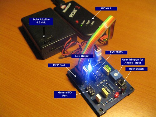
The Project Printed Circuit Board (PCB)
To make it more interesting I’ve designed the printed circuit board (PCB) and the schematic in the EAGLE v5.2.0 format for the Microchip PIC12F683 microcontroller project which you can download from here. The following picture shows the PIC12F683 microcontroller board used in this project:
Downloading the HEX Code
After compiling and simulating your code it’s time to download the code using the Microchip PICKit2 programmer, connect the PICKit2 ICSP (Microchip In Circuit Serial Programming) port to your PIC12F683 microcontroller pins then from the Programmer menu Select Programmer -> PicKit2; You will get this following result on the output windows of the Microchip MPLAB IDE:


Now its time to watch your Microchip PIC12F683 microcontroller “Reading the Port” Assembler Programming:
The Final Thought
With 15 Microchip PIC assembler instructions you’ve just learned, actually it’s almost cover all the basic PIC assembler instructions needed to build a complex application and learning the remaining PIC instructions is not much harder that what you’ve already learned on this tutorial. Always practicing and reading the PIC assembler code made by other peoples; hopefully this will give you a solid understanding of how to program in PIC assembler language.
Bookmarks and Share


